- 您现在的位置:买卖IC网 > Sheet目录287 > 25LC040AT-E/MC (Microchip Technology)IC EEPROM 4KBIT 10MHZ 8DFN
25AA040A/25LC040A
2.7
Data Protection
2.8
Power-On State
The following protection has been implemented to
prevent inadvertent writes to the array:
? The write enable latch is reset on power-up
? A write enable instruction must be issued to set
the write enable latch
? After a byte write, page write or STATUS register
write, the write enable latch is reset
? CS must be set high after the proper number of
clock cycles to start an internal write cycle
? Access to the array during an internal write cycle
is ignored and programming is continued
The 25XX040A powers on in the following state:
? The device is in low-power Standby mode
(CS = 1 )
? The write enable latch is reset
? SO is in high-impedance state
? A high-to-low-level transition on CS is required to
enter active state
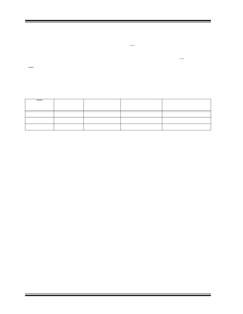
TABLE 2-4:
WRITE-PROTECT FUNCTIONALITY MATRIX
WP
(pin 3)
0 (low)
1 (high)
1 (high)
WEL
(SR bit 1)
x
0
1
Protected Blocks
Protected
Protected
Protected
Unprotected Blocks
Protected
Protected
Writable
STATUS Register
Protected
Protected
Writable
x = don’t care
DS21827G-page 12
? 2003-2011 Microchip Technology Inc.
发布紧急采购,3分钟左右您将得到回复。
相关PDF资料
25LC080A-I/STG
IC EEPROM 8KBIT 10MHZ 8TSSOP
25LC1024T-E/MF
IC EEPROM 1MBIT 20MHZ 8DFN
25LC128-E/MF
IC EEPROM 128KBIT 10MHZ 8DFN
25LC160/P
IC EEPROM 16KBIT 2MHZ 8DIP
25LC160B-I/PG
IC EEPROM 16KBIT 10MHZ 8DIP
25LC256T-E/MF
IC EEPROM 256KBIT 10MHZ 8DFN
25LC320A-I/P
IC EEPROM 32KBIT 10MHZ 8DIP
25LC512-E/MF
IC EEPROM 512KBIT 20MHZ 8DFN
相关代理商/技术参数
25LC040AT-E/MNY
功能描述:电可擦除可编程只读存储器 4K 512 X 8 2.5V SER EE EXT RoHS:否 制造商:Atmel 存储容量:2 Kbit 组织:256 B x 8 数据保留:100 yr 最大时钟频率:1000 KHz 最大工作电流:6 uA 工作电源电压:1.7 V to 5.5 V 最大工作温度:+ 85 C 安装风格:SMD/SMT 封装 / 箱体:SOIC-8
25LC040AT-E/MS
功能描述:电可擦除可编程只读存储器 4K 512X8 2.5V SER EE EXT RoHS:否 制造商:Atmel 存储容量:2 Kbit 组织:256 B x 8 数据保留:100 yr 最大时钟频率:1000 KHz 最大工作电流:6 uA 工作电源电压:1.7 V to 5.5 V 最大工作温度:+ 85 C 安装风格:SMD/SMT 封装 / 箱体:SOIC-8
25LC040AT-E/OT
功能描述:电可擦除可编程只读存储器 4K 512X8 2.5V SER EE EXT RoHS:否 制造商:Atmel 存储容量:2 Kbit 组织:256 B x 8 数据保留:100 yr 最大时钟频率:1000 KHz 最大工作电流:6 uA 工作电源电压:1.7 V to 5.5 V 最大工作温度:+ 85 C 安装风格:SMD/SMT 封装 / 箱体:SOIC-8
25LC040AT-E/P
制造商:MICROCHIP 制造商全称:Microchip Technology 功能描述:4K SPI Bus Serial EEPROM
25LC040AT-E/SN
功能描述:电可擦除可编程只读存储器 4K 512X8 2.5V SER EE EXT RoHS:否 制造商:Atmel 存储容量:2 Kbit 组织:256 B x 8 数据保留:100 yr 最大时钟频率:1000 KHz 最大工作电流:6 uA 工作电源电压:1.7 V to 5.5 V 最大工作温度:+ 85 C 安装风格:SMD/SMT 封装 / 箱体:SOIC-8
25LC040AT-E/ST
功能描述:电可擦除可编程只读存储器 4K 512X8 2.5V SER EE EXT RoHS:否 制造商:Atmel 存储容量:2 Kbit 组织:256 B x 8 数据保留:100 yr 最大时钟频率:1000 KHz 最大工作电流:6 uA 工作电源电压:1.7 V to 5.5 V 最大工作温度:+ 85 C 安装风格:SMD/SMT 封装 / 箱体:SOIC-8
25LC040AT-H/SN
功能描述:电可擦除可编程只读存储器 4K, 512 X 8, 2.5V SER EE 150C RoHS:否 制造商:Atmel 存储容量:2 Kbit 组织:256 B x 8 数据保留:100 yr 最大时钟频率:1000 KHz 最大工作电流:6 uA 工作电源电压:1.7 V to 5.5 V 最大工作温度:+ 85 C 安装风格:SMD/SMT 封装 / 箱体:SOIC-8
25LC040AT-I
制造商:MICROCHIP 制造商全称:Microchip Technology 功能描述:4K SPI Bus Serial EEPROM